
Vintage Chips
For historical reasons I keep some rare vintage chips from the past despite I do not need them.
| Name | Amount | Purpose of chip | Comment |
|---|---|---|---|
| AM9149-70DC | 12 | Early SRAM from AMD. 18 Pins in a ceramic DIP. I did not found any description for the AM9149 on the internet. What I’ve found was a description for AM9111 and for AM9150. The AM9111 has also 18 Pins like the AM9149, so I bvelieve the AM9149 is close to that chip. “-70” means access time 70ns. ( The AM9150 has 2Kx4 and 24 Pins). AM9111 is a 256x4 Bit Static RAM. Below is a picture of the AM9111 taken from the datasheet as of 1986. 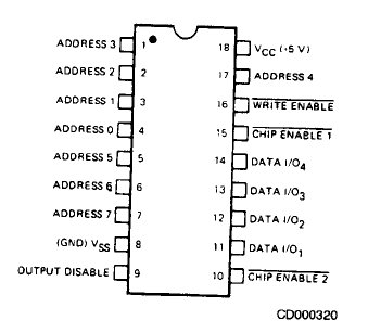 |
Data sheet from 1986 |
| AM27LS01PC | 15 | Early 256x1 Bit SRAM, Open Collector. 16 Pins plastic DIP. I found only an excerpt of the datasheet in Internet describing the 27LS08 and 27LS00. The complete document is named “Advanced Micro Devices -Schottky And Low-Power Schottky Bipolar Memory, Logic and Interface”, 1975. | Data sheet from 1975 |
| AM27LS02PC / AM27LS02APC | 15 / 2 | 64 Bit SRAM 16x4, Open Collector. 16 Pins plastic DIP. The complete document describing this chip is named “Advanced Micro Devices -Schottky And Low-Power Schottky Bipolar Memory, Logic and Interface”, 1975. | Data sheet from 1975 |
| 10124N | 2 | Quad TTL/DTL-Input Level Translator. Chip made by Signetics, 16-pin plastic DIP. Chip print says: 10124N 8201 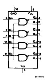 |
Data sheet from 1986 |
| 6308-1J | 1 | Fuse-Programmable PROM, 256x8. Chip made by Monolithic Memories (MMI). 20 pin ceramic DIP. Chip print says: 6308-1J 8208 | A chip from the 1980ies. One-Time programmable and already used, so it is of no practical use today. |
| 8304BN | 2 | Octal Three-State Bidirectional Bus Transceiver. Chip made byNational Semiconductor. 20 pin plastic DIP. Chip print says: 8037B DP8304BN INS8208BN and B8221 DP8304BN INS8208BN  |
A chip from the 1980ies |
DEC Chips
Some DEC chips, from an DEC LA120 Printer board. The LA 120 was a printer for the DEC PDP 11:
| Name | Amount | Purpose of chip | Comment |
|---|---|---|---|
| SN75189AN | 2 | Quad Line Transceiver (RS232) | — |
| DM81LS97N | 1 | Three-State Octal Buffers | — |
| DEC1488L | 1 | Line/Bus Transceiver? | — |
| DS8640N | 1 | Quad NOR Unified Bus Receiver | — |
| DC950 | 2 | ? | — |
| ER1400 | 1 | NV RAM ? | — |
Inside an old ROM chip
I have opened one of my 6308s and looked at it with a microscope. Below are some images made.
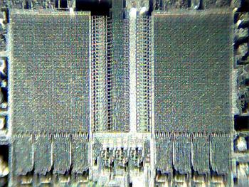
The ROM is obviously organized in two “banks”.
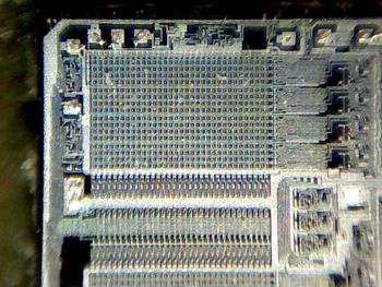
Closer Look to one bank (chip rotated -90 degrees in this picture). The big areas at the top are the connection points to the outer pins. Each “bank” has 16x32=512 black areas.
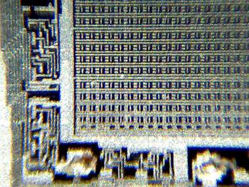
Even closer look to the elements that store the bits. My suspection: There are black areas containing two horizontal small lines, these areas are divided from each other by a small vertical line. Each of these areas must be able to hold 2 bits,because each “bank” has 16x32=512 of these areas, so both banks have 1024 areas and for the 256x8=2048 Bits the PROM offers we must be able to fill 2048 bits in the 1024 areas. In other words, each small horizontal line represents a bit. (Also interesting: In one corner of the chip there can be seen a “(C)” and some number (this is not shown here)).