
SoftTek - Eclipse-based control and visualization for measurement equipment
Note: this is work in progress. The software described is in development and not finished.
Note 2: This project was abandoned in the past; source code is still available here: https://github.com/DennisD2/wormhole
SoftTek is an Eclipse based application that is able to communicate via GPIB with some (vintage) measurement equipment of the Company Tektronix for control of the device and for visualization of measurement data.
Supported devices
The following devices are supported:
- Tektronix 1241 Logic Analzer (tested)
- Tektronix 1240 Logic Analyzer (not tested)
As far as I know, the 1240 and the 1241 are identical except that 1241 offers a color screen, 1240 is monochrome only. So in the following text, I will always use “1241” because I own that one, but the text is also valid for the 1240. To be more precise here, the EPROMs on the analyzer pcbs have mostly identical stickers for 1240 and 1241. The only difference known by me is that the character set of the 1240 and the 1241 are slightly different. The colors are coded into the byte value for a character, I do not know what a 1240 will display if it shall display a e.g. green ‘A’. Maybe even this makes no difference, if e.g. the color coding is interpreted as “highlighting” on the 1240. This would need further reading in the documentation…
Implemented features, missing features
SoftTek can…
- Load memory images from Tek device (setup images, acquisition images, reference memory images, rampack data)
- Display loaded data in a nice way (scaling, color coding, selection of groups
to display). All 72 channels in all groups can be displayed in one big
canvas (as apposed to the monitor view of the Tek 1241)
- Non-gliched and glitched data
- Chained data
- Display up to two time cursors to analyze displayed data
- Load and save device data to PCs harddisk
The implementation does not contain (why) …
- Ability to download memory images to the device (GPIB module is not yet capable of doing this, needs update of the AVR firmware used in my GPIB module, this is not related to the software SoftTek)
- No two timebase support and thus no multiplexing support (too complicated, needs more reading in the manuals)
- Not tested:
- synchronous mode,
- chained 18 bit channels (never needed),
- Chains with more than two cards (have only 2 9 channel and 2 18 channel cards, so my maximum is 2 card chains)
Requirements to run the software
- Java JRE 1.6 or higher. Tested with 1.6.
- Currently, only Linux support, no Windows-plattform incarnation of the Eclipse RCP (I have no Windows PC to test with)
- Some GPIB controller attached to the device and attached to the PC where this software is running on. I used for my purposes my own Implementation of a GPIB-Controller running on an AVR board. This board is attached to the PC via RS232. A description of this device can be found here [3]
The Tek 1241
Some information on the device to enable understanding of the software. A more general intro to the 1241 is given in [2].
The analyzer supports up to 72 channels. It is able to view signals in state diagrams and in timing diagrams.
It supports frequencies up to 50 Mhz (synchronous) and 100Mhz asynchronous. The device has 2 time bases and offers 15 levels of trigger conditions. The two time bases allow e.g. a slow clock on the first time base to get some first trigger close to the area that shall be analyzed and then a high frequency clock for the second time base to get a much finer view into the area to be analyzed.
The organization of the input side of the device is as follows:
- There are 4 lines for slots at the right side of the device. For each line, two slots are possible. These slots are numbered 0,1 for first line, 2,3 for second line, 4,5 for third line and 6,7 for fourth line.
- There are 9 channel and 18 channel acquisition memory cards. A 9 channel card uses a single slot (e.g. 0 or 2), an 18 channel card uses two slots (e.g. 4+5 or 6+7). These cards are located inside the device.
- A Pod is a probe with 9 data input lines (and one clock/qualifier input line for e.g. synchronous mode). The Pod is external to the device and is attached via a cable and a connector into a acquisition memory card.
- Between a Pod and the device under test, a lead set needs to be used. The lead set can be attached to the pod and offers e.g. micro clamps to attach the data input line to the device under test.Each Pod also has an “Id-Button” that produces a screen read out of the pod id.
For my device:
| Slot | Card |
|---|---|
| 0 | 9 channel |
| 1 | - |
| 2 | 9 channel |
| 3 | - |
| 4 | 18 channel (card 1) |
| 5 | 18 channel (card 1) |
| 6 | 18 Channel (card 2) |
| 7 | 18 Channel (card 2) |
My device has two 9 channel cards and two 18 channel cards. The two 9 channel cards are located in slots 0 and 2. The two 18 channel cards are located in slots 4+5 and 6+7. I have in total 6 pods of type 6460 which allow together with 9 channel acquisition cards to control the logic threshold (signal level threshold for separating HI and LO on a line). 18 channel acquisition cards have always fixed TTL level threshold.
In the analyzer, a Test Pattern Generator TPG is built in. This generator creates well defined sequences of patterns. There are two 9 channel wide pattern sequences. To easily use the TPG, a test lead set was provided by Tektronix.
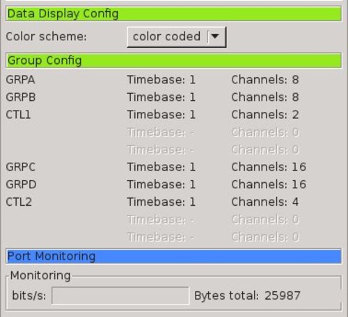
Display Groups
Display groups are used to do a grouping of input data lines for display. E.g. one group can contain data bus lines called e.g. “D0-D8” and another group can contain some lines to monitoring an SPI communication. Grouping is done by the user and includes naming the group, assigning a timebase and other things.
The Analyzer has a default grouping at startup. This depends on the aquisition cards inserted. For my device:
GRPA Pod 0, Bits 0..7 GRPB Pod 2, Bits 0..7 CTL1 Pod 0, Bit 8 Pod 2, Bit 8 GRPC Pod 4, Bits 0..7 Pod 5, Bits 0..7 GRPD Pod 6, Bits 0..7 Pod 7, Bits 0..7 CTL2 Pod 4, Bit 8 Pod 5, Bit 8 Pod 6, Bit 8 Pod 7, Bit 8
Grouping is part of the setup. Setups can be stored in a ROMPACK if available or in a NVRAM area of the analyzer.
There is much more to say on the 1241, see e.g. the user manual.
Theory of Operation of SoftTek
The 1241 can communicate with a controlling PC via a GPIB controller (if equipped with a GPIB interface module) or via RS232 (if equipped with a RS232 module). My description is based on the GPIB module approach.
For short pieces of textual information, the information is exchanged between a Controller/PC and the 1241 in human readable strings.
Some of the data is large, of binary type and transfered in a data block-oriented format. This data include:
- Setup information
- Acquisition and Reference Memory content
- RAM- and ROM-Pack content.
The GPIB-Implementation of Tektronix for the devices is documented in [1]. The implementation defines “Data Blocks” and “Memory Images”.
A data block is a container with some header and trailer information surrounding a number of payload bytes. Seen from today, a data block is quite small (maximum payload 61 bytes). The payload bytes are encodings of binary data bytes. The 1241 is able to use three different data formats for the bytes:
- ASCII HEX: Each Byte is coded in two bytes, representing the hex value of the original byte. E.g. byte 0xa2 will be encoded as two ASCII chars ‘A’‘2’.
- TEK Binary: Each byte stands for itself. E.g. byte 0xa2 will be transfered “as is”, namely as byte 0xa2.
- IEEE728 Binary: Close to TEK Binary, but this is an IEEE standard for transferring binary data. The definition of IEE728 can be found somewhere in the Internet
Both binary encodings require a transport way that is able to transfer binary data, i.e. bytes with values >0x7f.
My implementation uses RS232 to connect the GPIB controller to the PC. The controller is homebrew, described in [3] and supports only XON/XOFF software handshake, so only ASCII (non-binary) data can be transferred via my implementation. So I am using the ASCII HEX type for the data blocks ( which is the default for the Tek 124* device). My implementation also include some code for binary formats, but this hasn’t been tested. Because the data size per memory image is not very large (some KBytes) it is ok to use ASCII encoding despite it needs nearly the double amount of bytes compared to a binary encoding.
A memory image is a sequence of binary data bytes. If the user requests the transmission of e.g. the acquisition memory via GPIB, the Tek device creates a memory image from its internal hardware memory. This memory image is then converted to a sequence of data blocks and sent to the controller. The controller transfers the data to the PC and there some software converts the data blocks back to the binary payload. By putting together the small binary payloads from the data blocks, the large memory image can be reconstructed in the PC.
The structure of the memory images is documented by Tektronix in [1], all values inside the image are defined by their offset in the memory image, their size and, of course, their meaning.
Implementation
The application is an Eclipse Rich Client. It uses a navigation view (left side of application) to display/modify configuration of the client and of the data from the 1241. It also has a big canvas that is used to display the timeline data.
My implementation offers at the bottom classes for data blocks and for memory images. The data block classes implement a reader interface. This interface encapsulates the reading method (ASCII HEX, binary). The memory image class defines methods to use a list of data blocks or a large sequence of ASCII bytes to build up the binary content of the image.
There are two implementations of the reader interface, to read data from the tek device, and to read data from files.
The communication to the Tek device uses a nice java implementation for serial connectivity, called RXTX from http://rxtx.qbang.org .
A class “Tek1241RawDevice” encapsulates all useful methods for the device and uses the memory images coming from the Tek device. Another class “Tek1241Device” uses a raw object (from class Tek1241RawDevice) to implement own logic above the raw calls. Both of these classes extend a class “AbstractRawDevice” resp. " AbstractDevice". If the software will be extended to other devices, these abstract classes are the point to extend from. To separate Raw classes from " Not-Raw" (cooked) classes: raw classes know about offsets in memory images and do access memory images to extract data from. Cooked classes are implemented on raw methods only and should not know about memory images.
The class “DisplayGroup” encapsulated all information about the “Group” objects from Tektronix that can be found in the setup memory image. The class “Channel” encapsulates information about a channel (to which pod and which bit inside the pod is this channel assigned etc.).
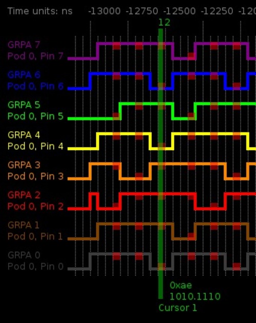
To have some interaction with the displayed data, I added a class “TimeCursor” which allows to create a set of cursors that can be moved on the data time lines to get the hex and binary values of the group data at a certain cursor position, like the screen cursor of the 1241.
The class NavigationView defines all UI elements at the left side and the menues.
The class View contains all methods to create, modify and display data in the big canvas area.
File format used
To store uploaded data on the disk of the PC, I “invented” a file format capable to store the acquisition data together with its setup data. Note that the acquisition memory image does NOT contain all the data to rebuild the complete information needed to load later on the device data, so we need the setup data valid during acquisition too. Example are all information about groups, which are stored in the setup image and not in the acquisition image. Because I had all the data available in the format that was sent by the device I decided to use that format. The data is in ASCII HEX format as described in the GPIB manual of Tektronix. Logically, the setup and the acquisition memory is each a (large) single line of ASCII characters. So my file format consists of fixed two lines:
- Line 1: Setup Information as raw ASCII HEX characters ending with a CR
- Line 2: Acquisition memory data as raw ASCII HEX characters ending with a CR
Because the data stored in the file is identical to the data read in by the device, it will be simple to download this data to the Tek 1241.
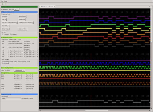
Screenshots
Below are some random screenshots showing the state of the work.
 Early version (03/2012)
 Early version; moved view to trigger event (red
line at position 0)
Early version; moved view to trigger event (red
line at position 0)
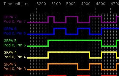
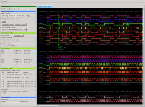
 Improved version with color coded timelines,
extraction of more information from memory images (April 9th 2012)
Improved version with color coded timelines,
extraction of more information from memory images (April 9th 2012)
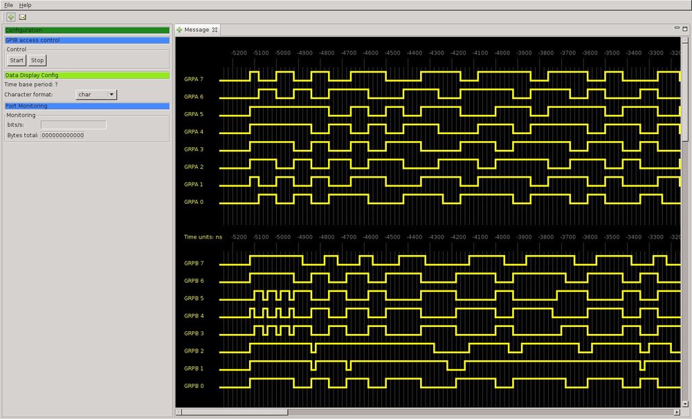
 Further improved version 04/2012
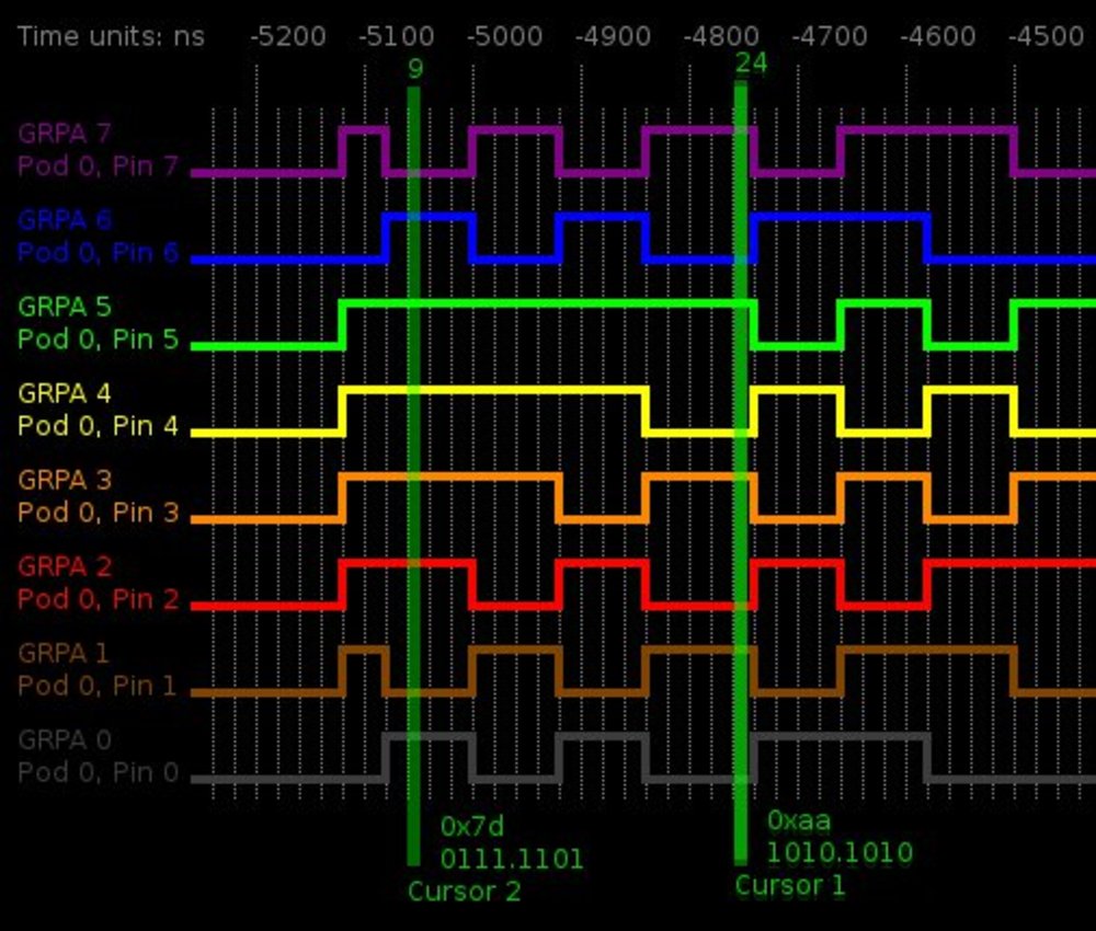 Closeup: the time cursors. They display in
numerical value the bit position and the hexadecimal and dual value of the Group
value (here it is a byte).
Closeup: the time cursors. They display in
numerical value the bit position and the hexadecimal and dual value of the Group
value (here it is a byte).
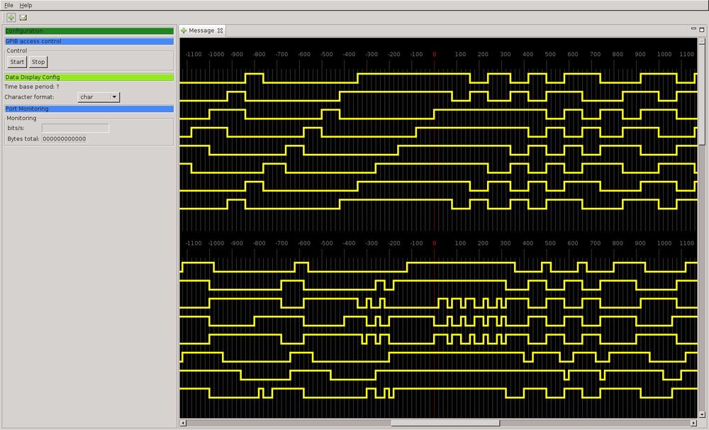
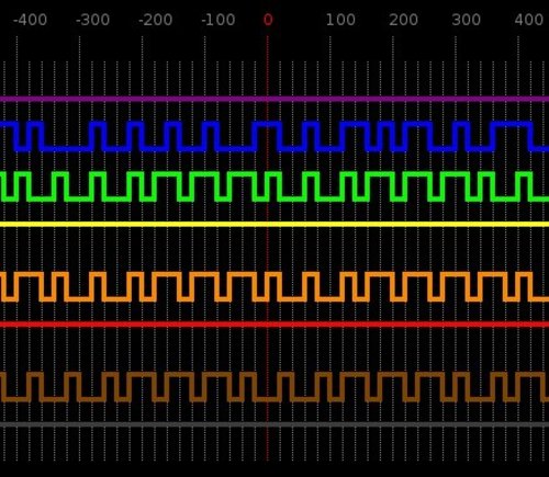 Look at the trigger position (red vertical line,
t=0)
Look at the trigger position (red vertical line,
t=0)
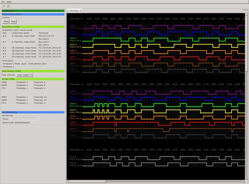
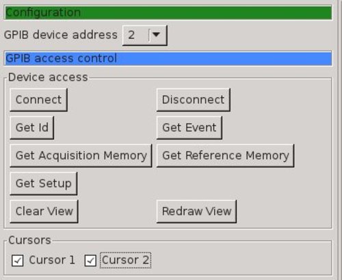 UI Elements for device access
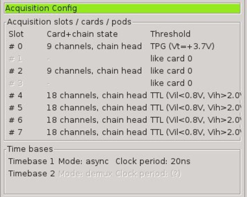 Info on aquisition capability of the device
 Some more info elements
 Display of data with glitches
 Closeup: display of data with glitches. A glitch (
the red area) means that there was at least one undisplayed transition between
the acquisitions before and after the glitch.
Closeup: display of data with glitches. A glitch (
the red area) means that there was at least one undisplayed transition between
the acquisitions before and after the glitch.
Examples for data files from a Tektronix 1241
Here are some examples of binary data coming from the 1241. All files are in ASCII HEX format:
- Content of the acquisition memory, contains 18 channels of capture data, captured with 20 ns asynchronous clock in ASCII HEX format (this is the result of a “ACQ?” GPIB query)
- Setup information used for the capture above (result of the “INS?” GPIB command)
- Content of a 64KB RAM pack (result of a “RAM?” command)
Source code
This project was abandoned in the past. Source code is still available here:
https://github.com/DennisD2/wormhole
Further information
[1] GPIB COMM Pack 1200C02, Tektronix, revised printing November 1986, downloadable via Internet
[2] Der Logik-Analysator Tekronix 1241, here
[3] Communication via GPIB with AVR, Description of my software-only implementation of a simple GPIB controller: here
[4] RXTX library for serial communication with Java. http://rxtx.qbang.org