
DEC PDP11 Rebuild
This document contains information I have gathered when trying to bring some DEC PDP11 boards together to have a “working” system.
Summary of boards
I have collected some boards in the last years.
CPU boards:
- M8186 LSI-11/23 CPU (C Revision, so capable of 22 bit addressing)
RAM boards:
- M8044 MSV11-DD 32K RAM, 18Bit
- M8067 512KB RAM, 22 Bit
Serial boards:
- M8028 DLV-11F serial board
- M3104 serial board
Multi Purpose Boards:
- M8047 MXV11-A Multi Purpose Card, 18 Bit.
Disk controllers:
- M8029 RX02 Disk Controller, 18 Bit
- EMULEX CS02H1 Controller.
Cages, Backplanes, Misc:
- H9278-A backplane
- BA11-MF mounting box with H9270-A backplane
- H780-F power supply
Power consumption in Ampere for some boards:
| Board | 5V | 12V |
|---|---|---|
| M8186 | >2 | 0.14 |
| M8044 | 0.96 | 0.07 |
| M8029 | 1.38 | 0.0 |
Minimal system
A minimal system would let the CPU boot up and enter the ODT debugger built into the CPU itself. The CPU would need RAM to execute code and a serial card for interacting with the user. This is not very useful, but already a complicated step.
Looking at my set of boards, I have several options for this minimal system.
I could use the multipurpose module M8047 and get this small system:
- M8186 CPU Board
- M8047 MXV11-A Multi Purpose Card, 18 Bit
But the multipurpose board has overwhelming 60 jumpers to configure all of its functions. This is too complicated for me in the first step. So I will try it with another configuration, that needs one card more. This system should be able to come up to ODT console:
- M8186 CPU Board
- M8044 MSV11-DD 32 KBytes RAM
- M8028 DLV-11F Serial Board
M8186 CPU jumper configuration
The CPU board has 18 jumpers to configure.
The purpose of the jumpers is described in KD11-AA User’s Guide, chapter 2.1.
The following table lists the values I think are needed in my configuration.
| Jumper | Purpose | O=Open, I=Inserted | Comment |
|---|---|---|---|
| W1 | Master Clock Enable | I | |
| W2 | Reserved | O | |
| W3 | Reserved | I | |
| W4 | Line Event O=enabled | O | Check later |
| W5 | Power Up Mode | I | see below |
| W6 | Power Up Mode | O | see below |
| W7 | Halt Trap O=enter ODT | O | Go to ODT on HALT |
| W8 | Bootstrapmode I=173000 | O | I do not want bootstrapmode |
| W9 | Bootstrap address | I | Not used |
| W10 | Bootstrap address | I | Not used |
| W11 | Bootstrap address | I | Not used |
| W12 | Bootstrap address | I | Not used |
| W13 | Bootstrap address | I | Not used |
| W14 | Bootstrap address | I | Not used |
| W15 | Bootstrap address | I | Not used |
| W16 | Reserved | I | |
| W17 | Reserved | I | |
| W18 | Wake up circuit 0=enabled | I | Check later |
W5, W6: Values I,O means console ODT. This is what I want.
W4: I keep it at O=Open, so the event is enabled. This event triggers an BEVENT interrupt in CPU, which executes the “line clock vector” at address octal 100. This can be used to implement a 60 Hz triggered real time clock. My hope is that this mechanism does not disturb the ODT.
W18: I keep it at I=Inserted. So that circuit is disabled. As far as I understood, the wake up circuit is for environments where unattended restarts need to be possible. So I guess it is ok to have this disabled.
For all jumpers with purpose Reserved, I have listed the factory defaults.
Some “Jumpers” are in reality 0 Ohms resistors or just soldered wires.
M8044 MSV11-DD RAM jumper configuration
My board is a M8044-DA , Module name MSV11-DD.
The RAM board has 5 jumpers to configure. In fact it has some more, but some are soldered and need no modification. Like battery backup use, bank 7 disable and parity config.
The remaining 5 jumpers do configure the start address of the RAM.
The purpose of the jumpers is described in LSI11 Systems Service Manual, page 487ff.
In a system with only this RAM, we can start RAM at address 0.
In this case, S1-1 …, S1-5 need to be set to N as can be seen in the manual N means On = closed. The opposite is F, which means Off = Open.
M8028 DLV-11F Serial Board Jumper Configuration
My board is a revision E with the newest chips on board 1985. This late revision is described well in Digital Microcomputer Interfaces Handbook, 1980 starting at page 201.
This board has a bunch of jumpers.
| Jumper | Purpose | O=Open, I=Inserted | Comment |
|---|---|---|---|
| A3-A12 | Bits A3..A12 of address word | =177560 | see below |
| V3-V8 | Vector bits A3..A8 | =60/64 | see below |
| R0-R3 | Rx baud rate bits | O,O,O,O | 19.200 baud |
| T0-T3 | Tx baud rate bits | O,O,O,O | 19.200 baud |
| BG | Break generation; if inserted break | I | allow break |
| P | Parity bit generation if inserted | O | No parity |
| E | Check for parity and generate parity bits | O | No parity |
| 1 | Number of data bits | O | 8 bits |
| 2 | Number of data bits | O | 8 bits |
| PB | Programmable baud rate if inserted | O | forbid first |
| C | Common speed op if inserted | I | |
| C1 | Common speed op if inserted | I | |
| S | Split speed op if inserted | O | |
| S1 | Split speed op if inserted | O | |
| H | Assert BHALT L bus line if inserted | I | |
| B | Negate BDCOK H bus line if inserted; puts CPU to HALT | O | |
| -B | Negate BDCOK H bus line if inserted; puts CPU to HALT | I | |
| 1A,2A,3A | Activate 20mA current Rx loop if inserted | O,O,O | |
| 1P,2P | Deactivate 20mA current Rx loop if inserted | I,I | |
| 4A,5A | Activate 20mA current Tx loop if inserted | O,O | |
| 3P,4P | Deactivate 20mA current Tx loop if inserted | I,I | |
| EF | Enable error flags to be read in high byte of Rx buffer if removed | I | disable first |
| M,M1 | Test jumpers for manufacturing | O,O | Do not touch |
| MT | Maintenance bit if inserted | O | Do not touch |
BG: Hope that generation of break signal does not disturb ODT
Baud rate: newer boards allow 19.200 baud
C,C1,S,S1: no split speed op. Both Rx and Tx have same speed
EF: disable error flag handling; hopefully has no effect
Changing jumpers
The jumpers are all wire-wrapped wires. I have no wire wrap tooling. Because many wires need to be removed and other wires need to be added, I do not want to do this without proper tooling. Nice thing is that wire wrapping seems to be a dead technique and I could get a used professional tool set for some few Euros on ebay.
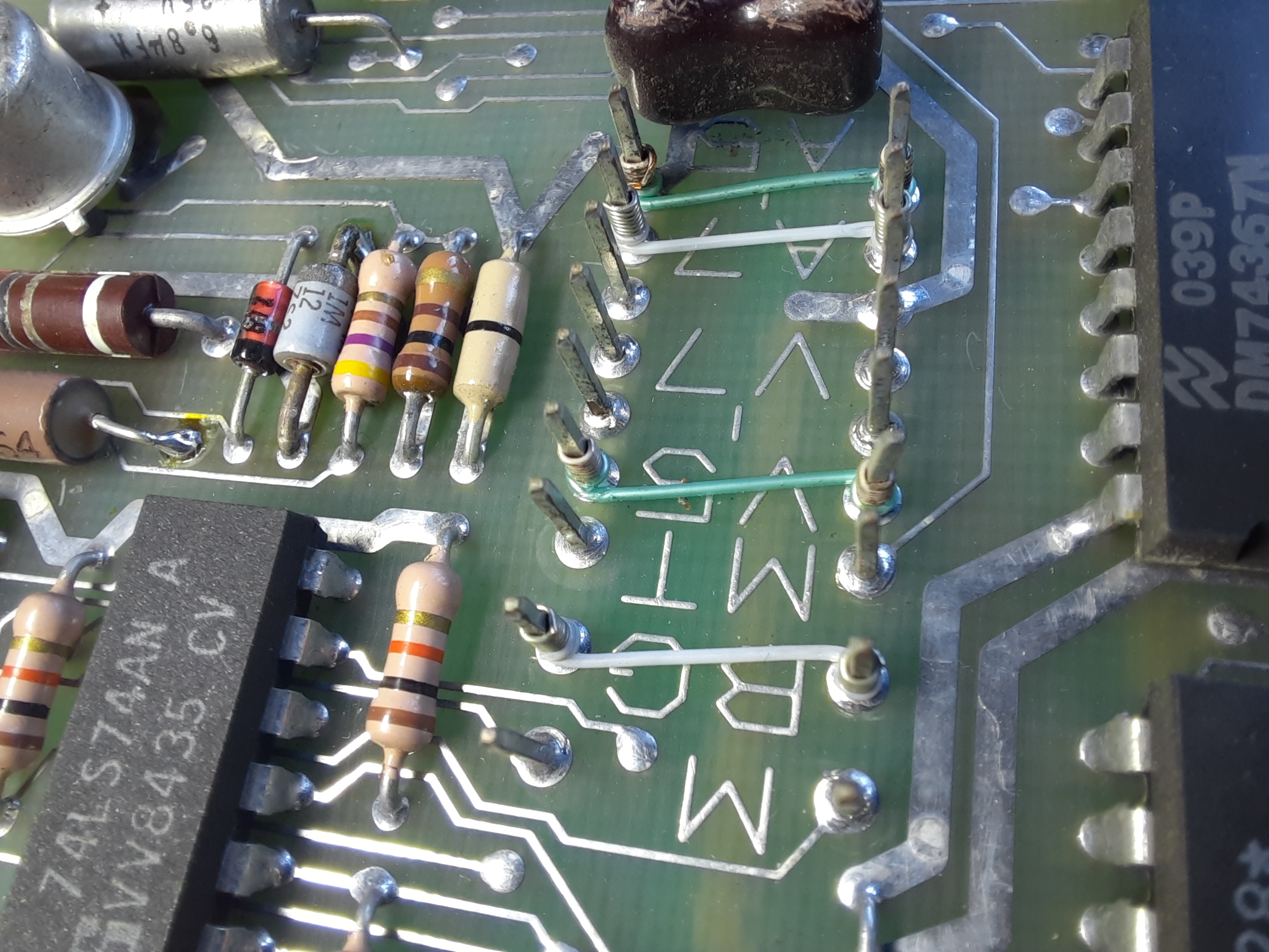
Image showing some of the jumpers, which are wire bridges in reality.
It needs some days until the tools arrive. In this time I will study what addresses A3-A12 and vector V3-V8 can be set.
How does addressing of a board work?
What I currently do not understand is, how the CPU finds a device board.
For accessing RAM board this is no problem, because RAM is there or not. CPU simply uses RAM by reading and writing from/to addresses in the address range. 0..(256-4)K.
I’ve read that upper 4K is reserved for external boards. The boards have some registers via which the CPU communicates with them. Boards appear at a base address and need some addresses to map in their registers. The base address can be set by jumpering some address bits, like A3-A12 for M8028. A13-A15 are always read as logical one. A0-A2 are used to address the board registers.
So this is all understandable. But how does the CPU finds the console device? Maybe console device has a well-defined, known base address. The same is maybe also true for the vector bits.
After some study I found this: Console needs to be present at fixed base address 177560 . Its 4 registers are at this and the three following addresses, last at 177566.
Standard vectors are RCSR=060 and XCSR=064 (receive and transmit).

Next I’ve created a three wire RS232 connection cable.
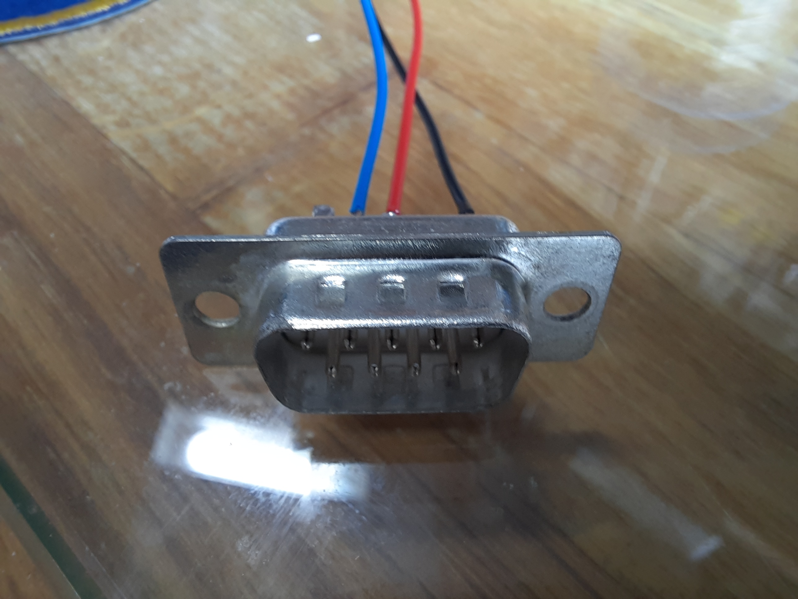
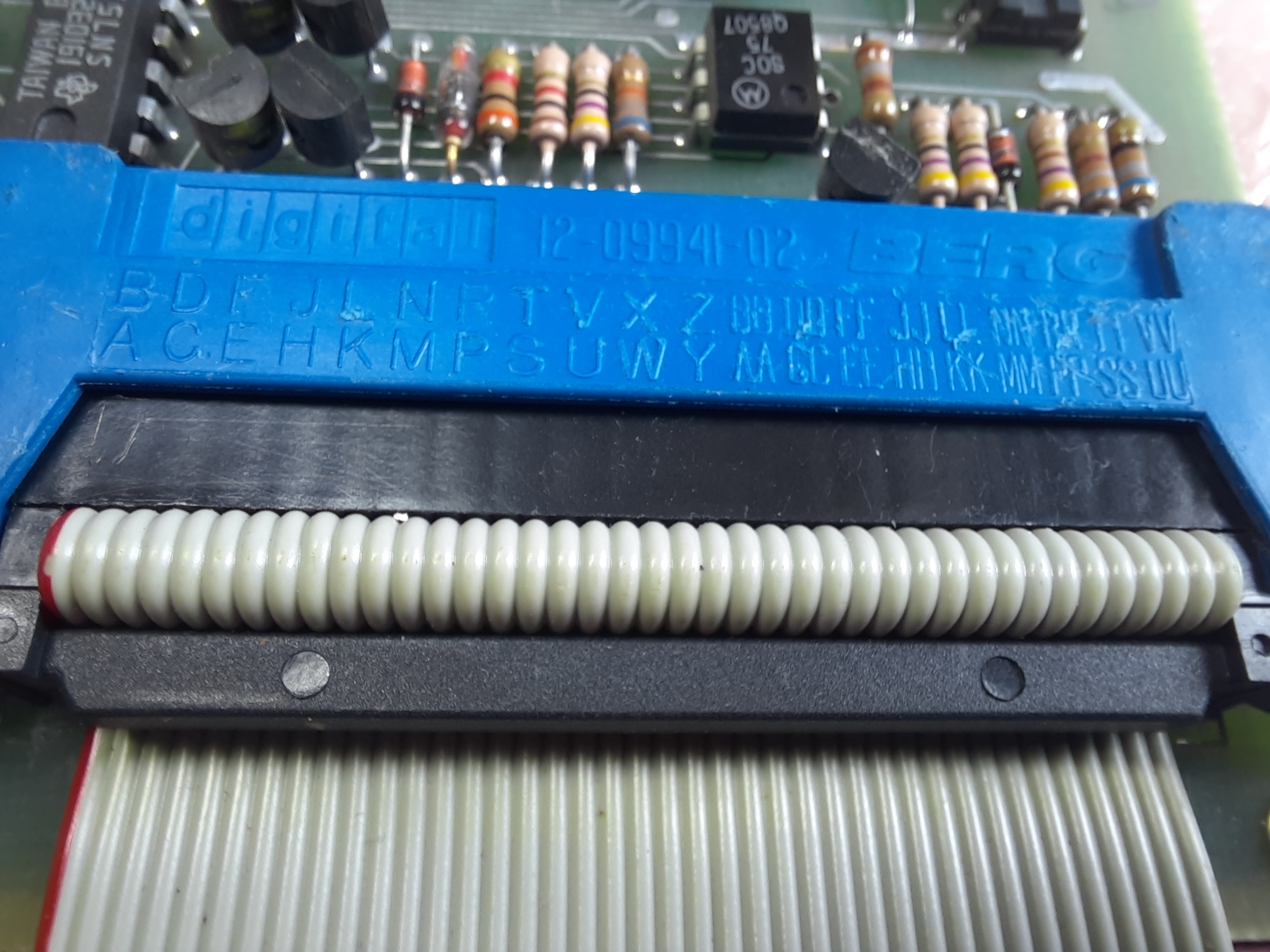
A standard 40 pin IDE connector fits into the BERG connector of the board. The nose at the plug needs to be removed, this can simply be done with a file. Connector is numbered from A to VV, as can be seen on next picture.
The connector looks a little over-engineered, because we need only three wires of the 40…
| BERG Pin | DEC Signal | IDE Pin | DB9 Pin (Null Modem) | DB9 Signal |
|---|---|---|---|---|
| E | EIA Interlock In | 36 | See below | |
| F | EIA Serial Out | 35 | 2 | RxD |
| J | EIA Serial In | 33 | 3 | TxD |
| M | EIA Interlock Out | 30 | See below | |
| VV | GND | 1 | 5 | GND |
The M8028 board requires that BERG Pin E and M are connected to work with EIA mode.
The information in the table comes from Minimal RS232 cable: KL8-E to 9-Pin DTE Device and https://homepage.divms.uiowa.edu/~jones/pdp8/hard8e/bc01v.html .
Switching on for the first time
Finally the wire wrap tools arrived.

Top: tool to remove isolation from wire, right Wrap/Unwrap tool, bottom left: Another tool to remove isolation from wire.
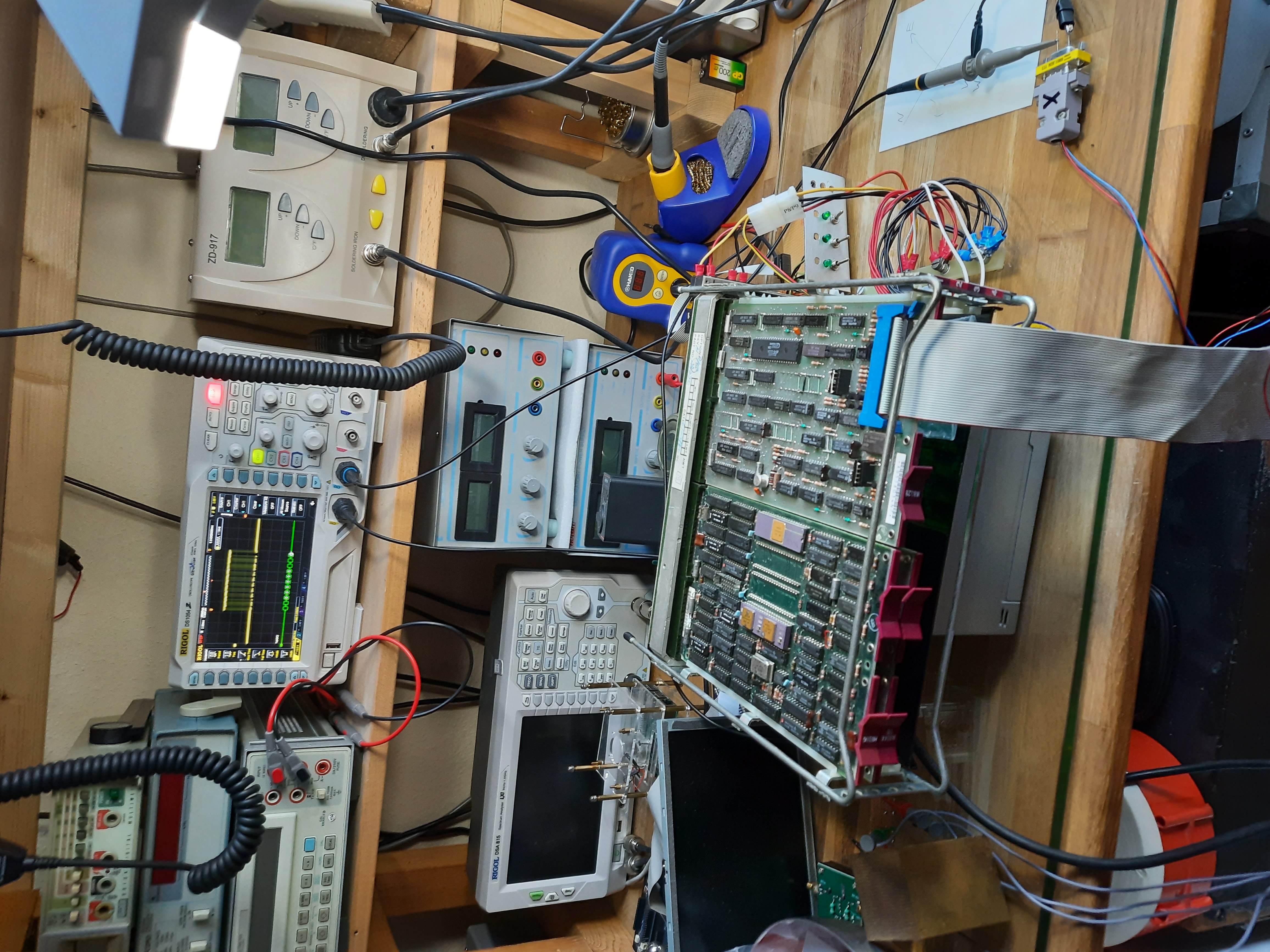
After having jumpered the CPU, the RAM and the serial board, I’ve switched on the whole system. Output of RS232 line was connected to an oscilloscope.
In my initial setup, I have the boards M8186 (CPU), M8028 (serial board), M8044 (RAM). All inside a BA11-MF housing. Power supply is from a PC PSU.
The oscilloscope in the background shows the first ASCII output of the CPU via serial board.
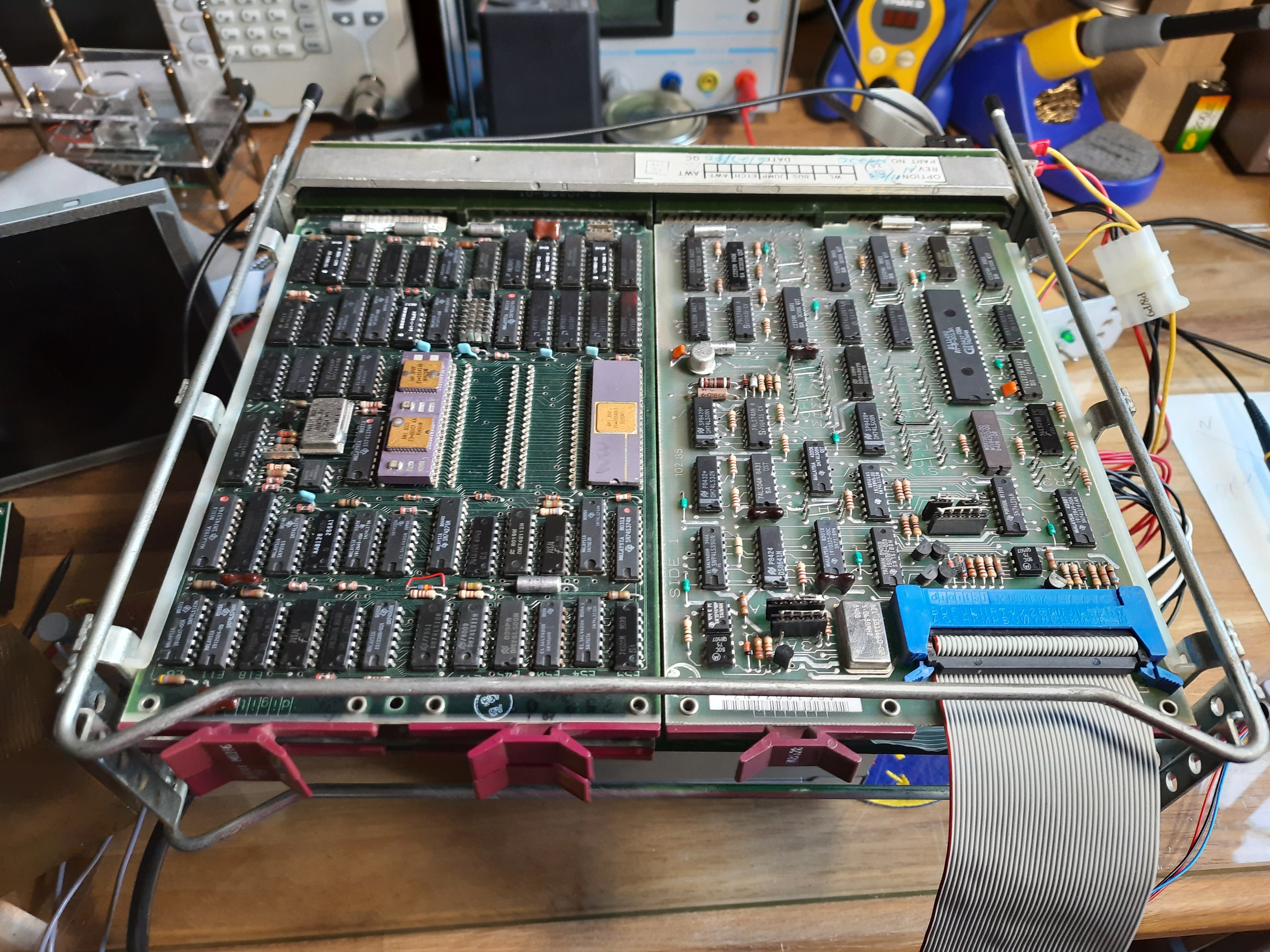
Closer look to the BA11-MF housing.
After some switching on and off: the scope catched the live sign of the system:
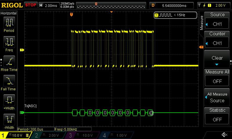
The yellow signal shows the raw RS232 signal levels. What can be seen in the green lower line is the decoded RS232 data:
000000
@
This is the correct output for a PDP11 CPU going to ODT (Online Debug Terminal).
After some trouble with connecting to the right wires, I managed finally to get the ODT also working with a Linux Terminal window running kermit.
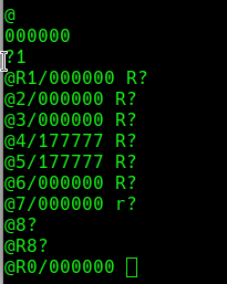
The command line always starts with @ created by the CPU.
After that commands can be entered. A valid command is
R0/. This prints out the content of CPU register R0 in the same line, directly after
the /.
Same command can be done for all registers R0..R7. R needs to be in
capital letters, as can be seen in the line where I tried r. CPU
immediately responds with a question mark. Next I entered a non-existent
register R8, resulting again in a question mark.
It is also possible to get the content of any RAM address, by entering
for example 1000/, which prints the content of that address 1000.
If the content has been printed out, it is possible to just enter a new value for that register or address. When hitting return key, the value then is written to register or address.
Using ODT, I was even able to verify that my RAM board is working.
SRUN bus signal is emitted by CPU if it is running, this means not in HALT/ODT mode. I have checked that signal, which is not a stable voltage but a periodic signal with about 600 Khz. See next image.
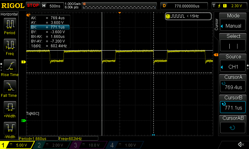
Above: SRUN signal while executing code. If The Enable/Halt switch is moved to Halt-position, the signal disappears, and the CPU enters Halt mode / ODT.
Some experiments with ODT, all copied from Diane Neisius page:
# "handle" traps
@0/176377 0
@2/000000
@4/177777 2
@6/000000
@10/177777 6
@12/000000
@14/177777 12

@242/000000
@244/177777 242

# init SP
@R6/000000 700

# Code that writes to RAM in a loop incrementing address
@1000/177677 5000 # clr r0
@1002/000000 5720 # tst (r0)+
@1004/177777 776  # br .-2
@1006/000000

# Execute that code, ends with "bus Error" trap at location 4
@1000G
000004

# Check result = last valid memory address + 2
@R0/160002
So my RAM board seem to have octal 160.000 addresses. This is 57.334 decimal or 0xe000. (64 - 8)K , 56K.
Hm. This result is somewhat confusing, because I thought that the RAM board has 32K Words (16 bit words). The result then should be something below 32.768 decimal. Strange…
I have to check this.
Time to rest
Bringing all the boards, bought over the years together into a system that is able to boot up until ODT, is a landmark on its own. To get there, I need to replace the not so well working power supply H780 with a PC PSU, and also to replace the Switch&Lights Boards (which is part of the H780 in case of the OBA-11MF) with an own solution took some days to bring everything together.
The final steps were supported by members of the great forum https://forum.classic-computing.de/. Many thanks to them.
So I will take a rest of some days before continuing in my rebuild. Next steps are already pointed out:
- replace the poor-wired RS232 connection with a better one (done)
- Add cooling fans to my build (done)
- Become familiar with ODT; There are some sites to check (done)
- Get closer to PDP11 assembler code (done. Erm. Ok yeah, not. To become really acquainted, could last a life. So not done but: Moved Forward.)
- Test out my second CPU board (done, does work after heavy cleaning)
- Test out my boardless PDP11 CPU I’ve got (done, chip is ok)
- New action item: Check what happened to my first CPU board (it broke, oh no, while I was typing). Where is my SALEA-Clone (what it has 8 bits only :-( ). And I sold my one hundred and what line Tektronix Logic Analyzer years ago… The HP Logic Analyzer also left. Puh. Hard work.
After these steps I want to:
- Try to get the complex board M8047 MXV11-A Multi Purpose Card working
- Connect a virtual tape drive running on my Notebook via M8047 board
- Boot RT-11 operating system from tape drive
- Do some assembler code programming using DECs Macro-11 assembler
- Make a virtual tape drive from an Arduino, a ATMega or an Raspberry, whatever is least effort
- Test out floating point unit
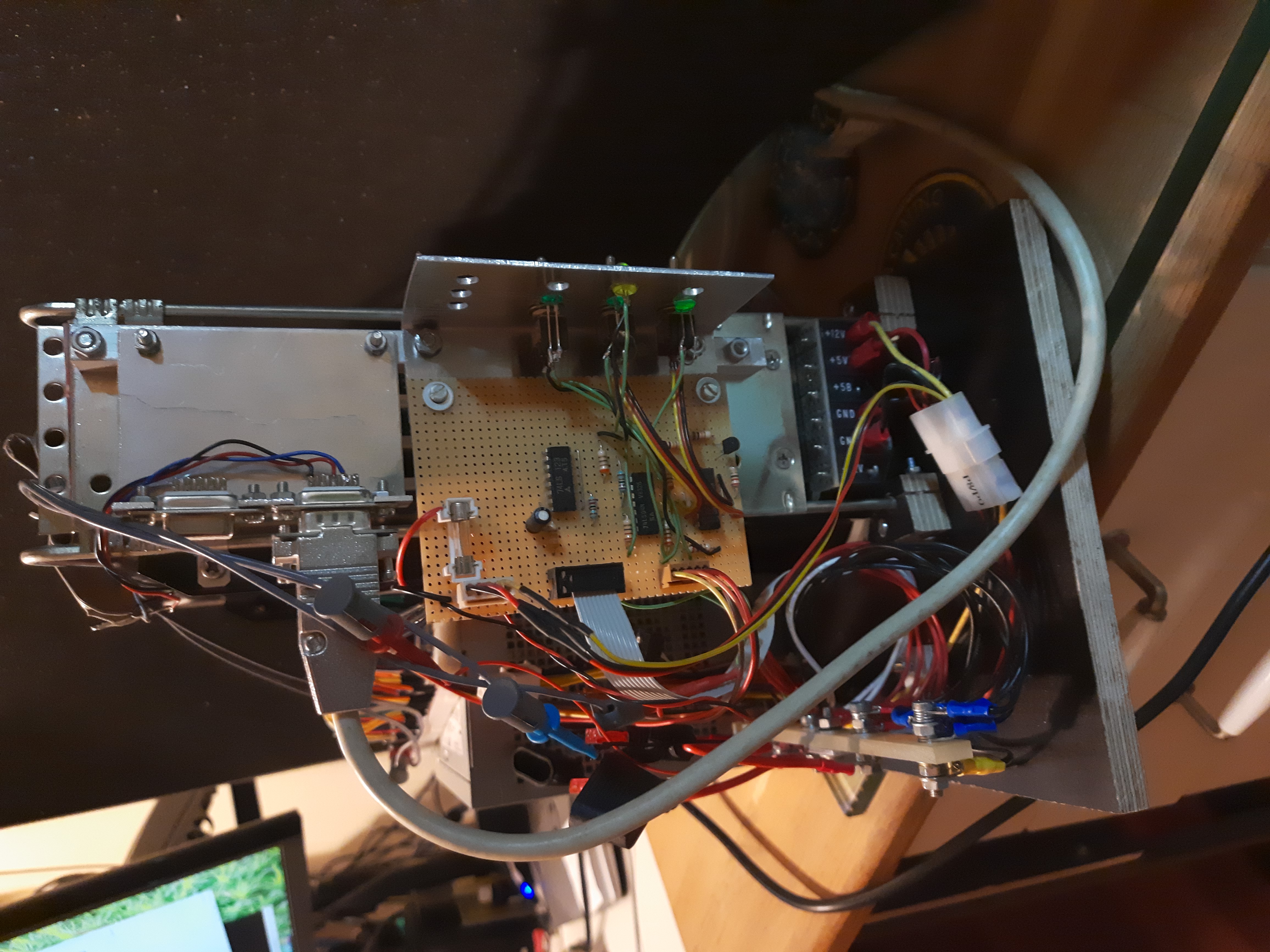
State reached as of end of year 2022
The BA 11-MC mounting box was mounted onto a wooden base plate to hold all the
parts together.
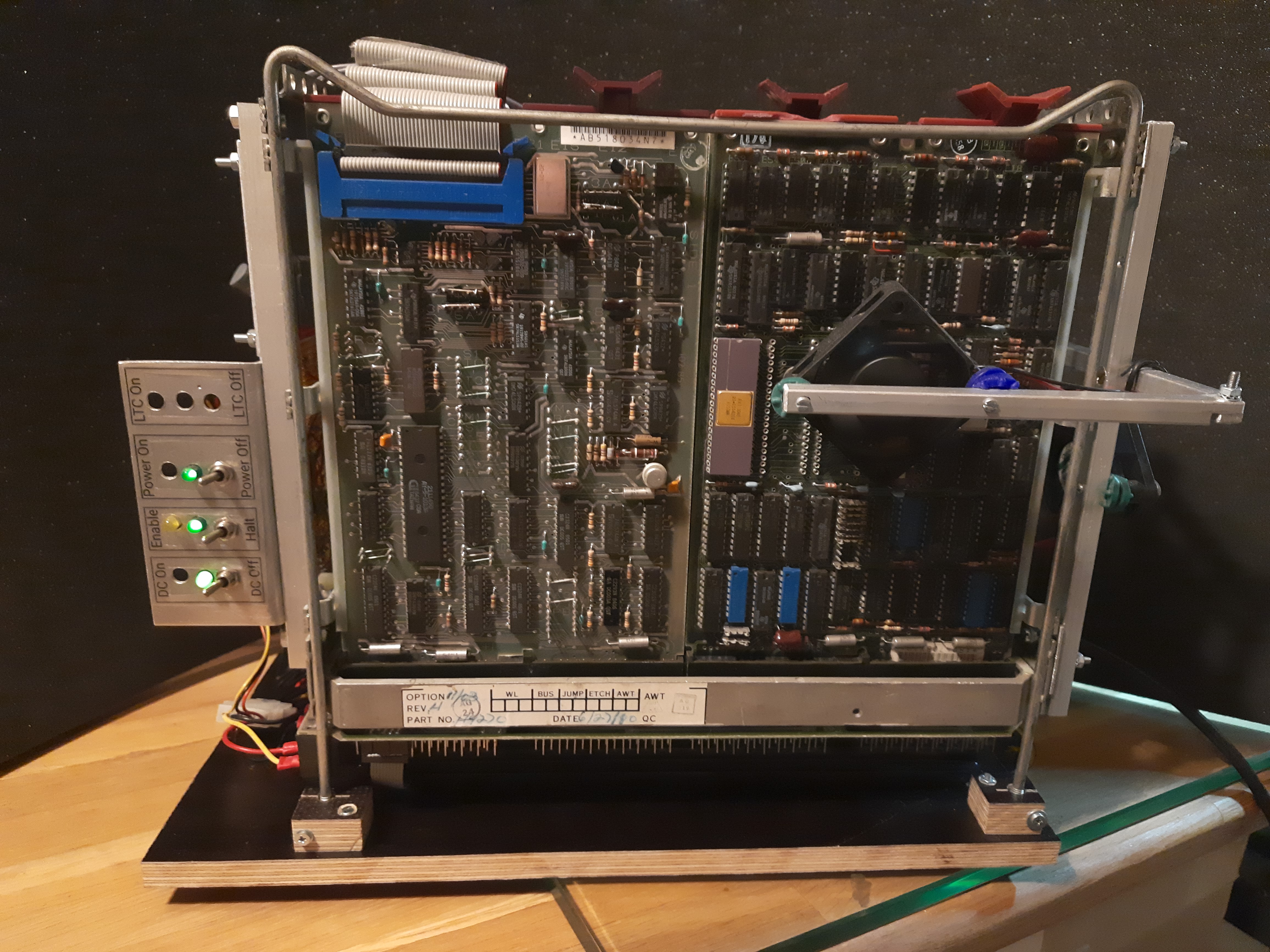
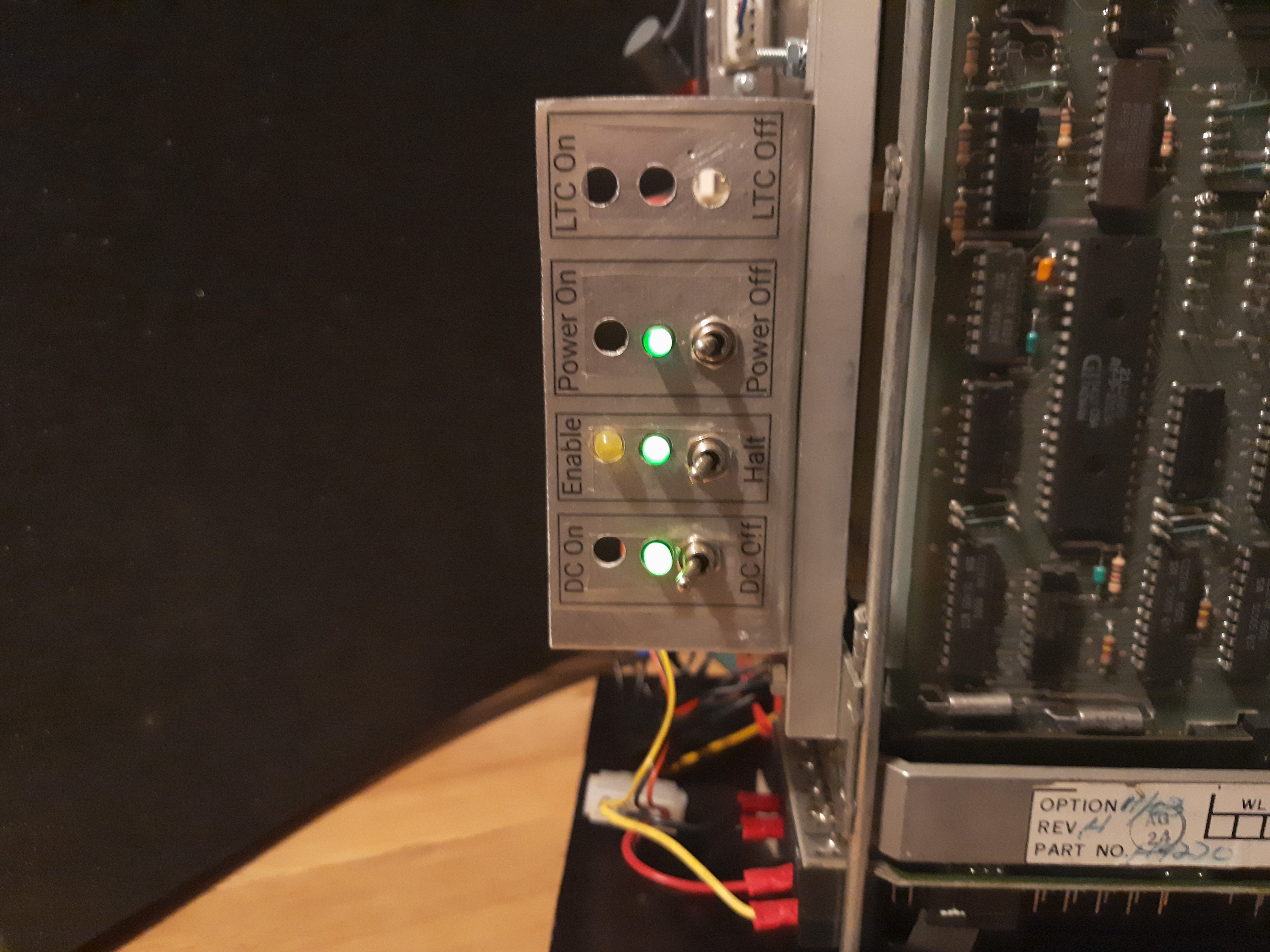
Self made simple switch/boot panel is shown below. The PC power supply has a soft power on. This function is connected to a button Power ON. After some settling time, the PC power supply signals stable DC availability on some output. I ignore this signal and have just another switch DC ON, that is connected to the PDP DC_ON input line. I rarely boot the thing, so this can be done manually. It would be very simple to wire the power supply output signal directly to the DC_IN line anyway. Last Button is Enable/Halt. Enable position is the common way to run the machine and allows free run and execution of code. Halt keeps the CPU in ODT mode which stops execution after each single step for debugging and other low level tasks.
View from right side. Two small fans run silently to keep the CPU cool.
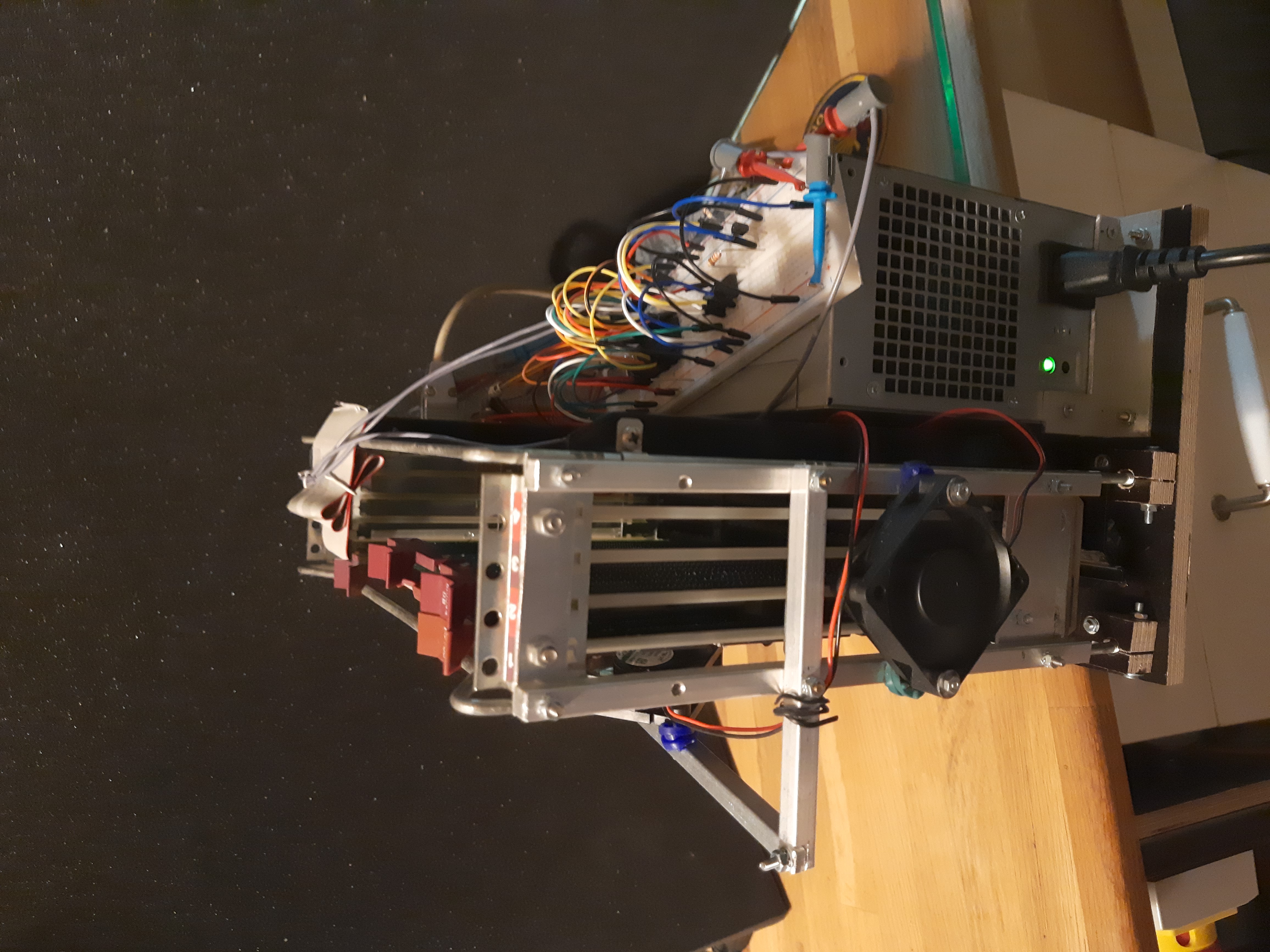
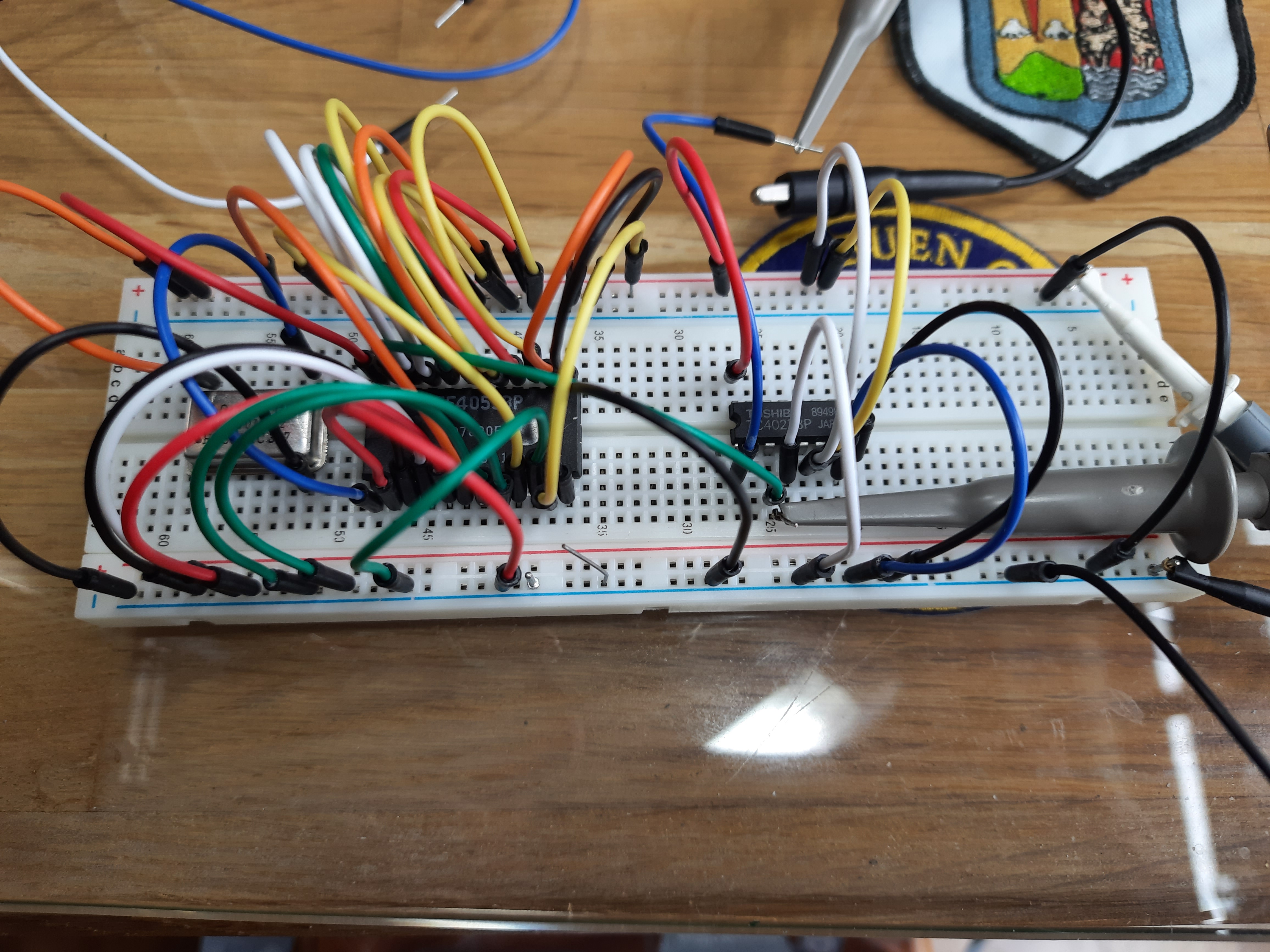
The breadboard visible contains a 50Hz quarz-controlled signal source with HEF4059
CMOS divider chip and a 1 Mhz quarz.The PC power supply is attached to base plate
with some screws.
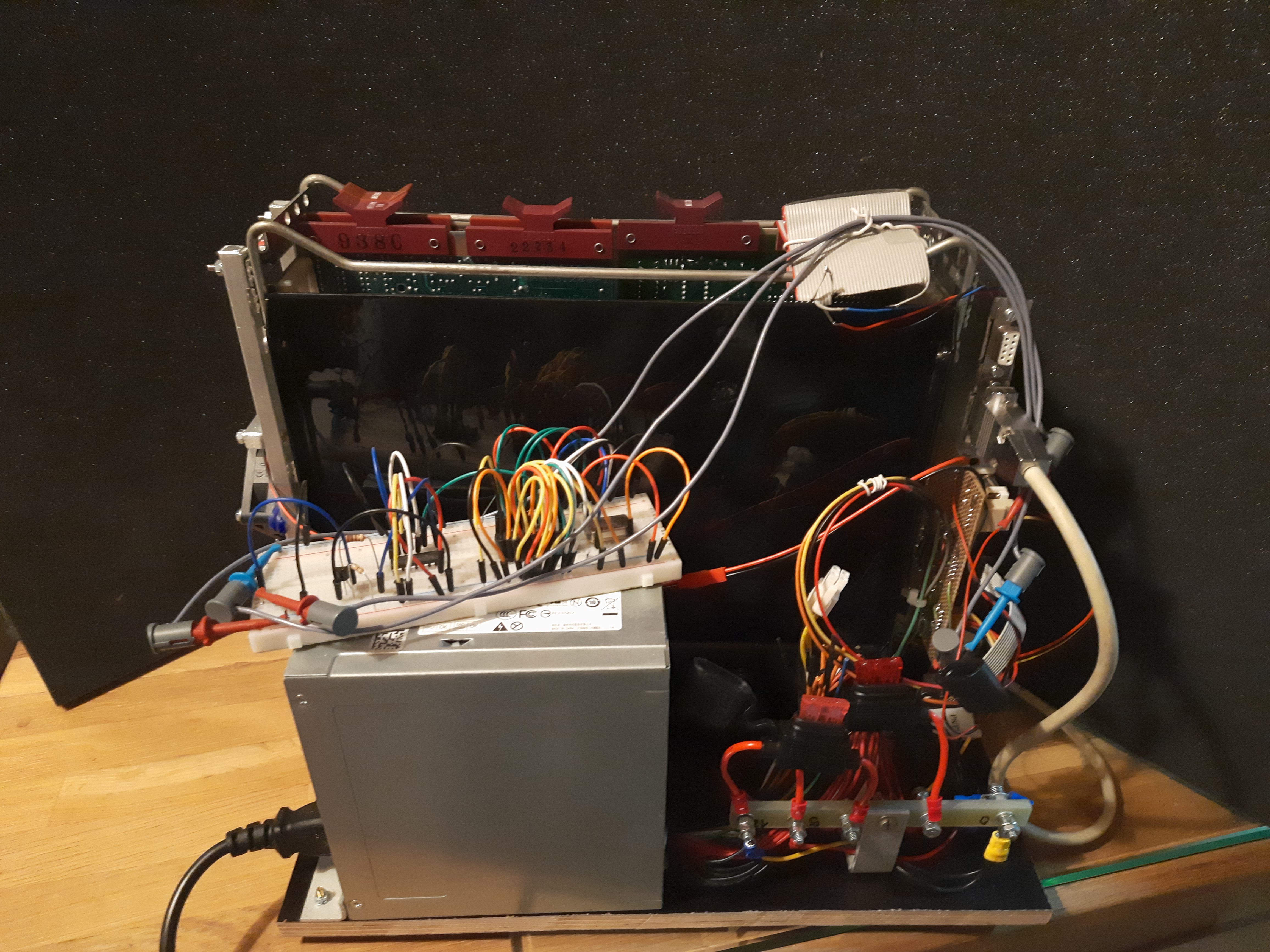
Self made control board for boot signals and the RS232 connectors.
View on 50Hz generator with HEF4059, a programmable divider chip. I divide the 1Mhz quarz signal with a divider of 10000, and have one additional flip-flop for the last division by 2. So the resulting frequency is 50Hz.
This signal is feed to PDP11 via the LTC signal line (Line Time Clock).)
Booting and connecting to PC: Connect RS232 to PC, 9600 Baud, 8N1.
Put all switches to off or halt. Put Power switch to on. Then put DC switch to on. On terminal, a @ should be written by PDP11.
To execute program code, always switch Enable/Halt button to Enable. Only then code can be executed.
If some program code runs in endless loop, code can always be interrupted by switching Enable/Halt button to Halt.
M8186 CPU board problems
The board I have used the first days suddenly stopped working. I have a second board, that is that what was part of the OBA11 machine. This also had contact issues in the beginning, and I switched the failing one with the second board.
The issue with the first board was, that it seems not to transmit data correctly. If I switch the machine on, then some well known characters should be sent to the console. But console gets only a SI,STX sequence. Because the serial board receives these characters, it was obviously correctly addressed, so I guess the addressing lines are all ok. But the data path somehow is faulty.
What a pity. I had a short look at the schematics of the CPU board, but this is a complex thing and would need MUCH more effort to trace the bug.
Let’s hope the second CPU board has no problems.
Further reading
https://www.pdp-11.nl/ - Great info and also software site